Passivation and Solder Mask
Copper corrodes quickly when exposed to oxygen. You must protect copper traces on outer layers from corrosion by passivation or by coating them with an inert material. Passivation refers to any treatment of the metal surface that renders it less reactive. For example, plating traces with tin or nickel produces a surface less susceptible to oxidation, but the extra thickness lowers the characteristic impedance of the trace. Pc-board fabricators normally compensate for the decrease in impedance by reducing the width of the etched trace before plating. As a result, for the same impedance, a composite plated structure never achieves as low a value of dc resistance as an unplated, bare copper trace.
These factors can also adversely affect the ac resistance of the trace, particularly if the plating material you use is a magnetic nickel alloy. Such materials suffer from a shallow skin depth and correspondingly large sheet resistivity at high frequencies, exaggerating resistive-trace losses. Commonly available 2-D electromagnetic-field solvers do not predict the amount of increase. Those tools assume you have enough sense to avoid nickel plating on long, high-speed traces.
Inert protective coatings serve a variety of purposes. They:
- Protect the copper traces from oxidation. You must passivate every exposed piece of metal that you can't protectively coat. Examples of structures requiring passivation include solder pads and edge-connector fingers.
- Protect the substrate from humidity. Most substrate materials readily absorb water vapor from the air. In epoxy-glass materials, the water vapor can enter microscopic interstitial voids between the glass fibers and the epoxy matrix, traveling great distances into the interior of the substrate. The water reduces the dielectric strength of the substrate and greatly increases its dielectric loss.
- Increase insulation resistance between traces. The inevitable accumulation of dirt and water degrades the insulation resistance between exposed metallic contacts on the surface of a board. In high-voltage circuits, it can cause arcing. An insulating coating covering the traces prevents conduction from one trace, through the dirt, to the next trace.
- Decrease spurious shorts between traces. During the reflow-soldering process, any water trapped within the solder paste explodes into steam, spewing tiny solder balls all over your board. If you cover the traces, the solder balls are less likely to short anything out.
- Control movement of solder during soldering. During reflow soldering, a via placed too close to a solder pad tempts the solder paste to slide over to the via and disappear down the hole. A thin line of solder mask drawn between the solder pad and the via acts as a solder dam, preventing the solder from moving to the via.
If you apply the inert coating before soldering, it is usually called a solder mask. Coatings you apply after assembly are conformal coatings. You may apply inert coatings either in sheet (dry) form or as a liquid.
Any coating increases the total mass of dielectric material near the trace, decreasing somewhat its characteristic impedance. Pc-board fabricators normally compensate for the decrease in impedance by reducing the width of the etched trace before plating, with a corresponding adverse impact on the dc and ac resistance.
All screened, curtain-coated, or dipped coatings flow in a viscous manner after application. Even if you initially apply them in a uniform thickness, after flowing, the material sags off the tops of traces, leaving a thinner coating on the top of each trace and pooling along the sides. The exact geometry of the coating, and therefore its effect on trace impedance, defies exact analysis.
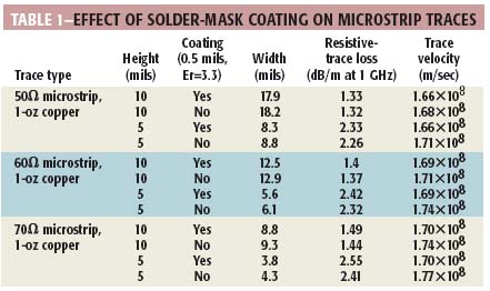
Table 1 lists the effect of a solder-mask overlay on a typical pc-board trace, assuming the coating is 0.5 mils thick with a dielectric constant of 3.3. For each combination of impedance and trace height, the table lists the trace width, showing the values required to obtain the stated impedance with and without the coating.
In each case, the coating slows the signal propagation by a small amount and increases the resistive-trace loss (because of the trace-width adjustment).