Jitter Reference Clock Settings
I've been writing about jitter for several years now, slowly putting together my thoughts in a logical sequence that I hope you find helpful. My first article about jitter was written in 2001, back when people still used a spectrum analyzer for what were then called phase-noise measurements. We've come a long way, and things are now much easier, but there are still some persistent little issues you need to know about. I'll be writing more about jitter later this year. Here's the collection of articles so far:
Jitter Reference Clock Settings
Let's set up a jittery clock waveform and attempt to measure its jitter.
As explained in my previous article, Jitter Capture, you cannot measure (or even define) the meaning of jitter in any absolute sense. All you can do is compare one signal against another and measure the difference in zero-crossing times between the two waveforms.
From that thought, the Jitter Capture article develops the key principle upon which all practical jitter measurements are based:
In the context of a serial data communication system, assuming that the receiver's PLL maintains lock, the main thing that matters in a receiver circuit, in terms of jitter, are the deviations that occur between the receiver's locally generated data recovery clock and the gyrations of the actual incoming data phase.
Applying that principle, if you wish to charcterize a signal under test, to determine if it will be acceptable to your receiver, you should set up a circuit like Figure 1.

Figure 1—Proper jitter characterization requires that the PLL settings within your test equipment match the settings in your receiver implementation.
This circuit first synthesizes from the signal under test a reference clock using the same type of algorithm that will ultimately be used in your finished system (same PLL gain and loop filter). The reference clock tracks much of the low-freuqency wander present in the signal under test, responding only to its remaining imperfections. Those imperfections, which appear as minute differences between the locally-synthesized reference clock and the signal under test, are called the local phase error. If you record the phase error in each cycle, you have made a phase track, as explained in the article Jitter Tracking.
Many digital scopes include built-in functions that automate the synthesis of a good reference clock and produce a phase track. This article illustrates features specific to the LeCroy family of digital oscilloscopes. Substantially similar features appear in high-end oscilloscopes availalble from other manufacturers.
Test Setup
I shall first create a test signal with a specific type of jitter.
The low-noise RF signal generator in Figure 2 creates a very pure 100-MHz sinewave carrier. A 6dB splitter combines (adds) to the 100-MHz sinewave a square-wave modulating signal. The period of the modulating signal is 1 usec (1 MHz), and its amplitude is a small fraction of the amplitude of the sinewave. The rise and fall time of the modulating signal is quick, but not so fast that it will ever produce a non-monotonic glitch near the zero crossings of the splitter output. The combined signal feeds to a pulse generator which squares up the signal present at its EXT gate, producing a digital output. The threshold of the EXT gate input is set to precisely 50%.
As measured at the output of the splitter, the modulating signal shifts the DC baseline of the RF signal up and down. Vertical shifts in the DC baseline change slightly the times of its zero-crossings, creating a subtle degree of phase modulation in the pulse generator output. The pulse generator output is coupled to the scope input channel four (CH4).
The amplitude of the modulated signal is set to create plus and minus 0.05 unit intervals (±50 mUI) of phase modulation at CH4. The scope operates in CLK mode, meaning that it registers only the positive edges of the input signal. One unit interval therefore equals 10 ns.
The signal at CH4 is, for the purposes of our discussion, the "signal under test".
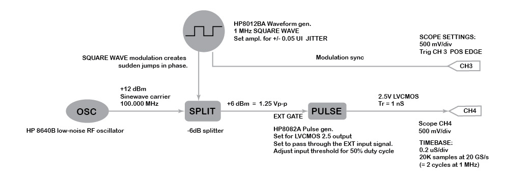
Figure 2—A 6dB splitter combines (adds) a 100 MHz RF carrier with a square-wave modulating signal to produce a phase-modulated clock at CH4. Click to enlarge...
Received Signal Processing
To the signal received at CH4, the scope applies an internal digital filter ERES+3 (Figure 3). This filter samples the input at a very high rate, but low-pass filters the output for the purpose of attenuating high-frequency white noise present in the scope input circuitry. Since the input signal carrier operates at the rather pedestrian rate of only 100 MHz, and the scope sampling circuits operate at 20 GS/s, a substantial degree of noise reduction is possible using this filtering technique.

Figure 3—Four distinct phase track generators process the input signal, creating four distinct phase tracks. Click to enlarge...
The filtered clock signal couples internally through the scope function F8 to four distinct processing blocks called "TIE@level" functions (P3-P6). You can think of each TIE@level function as a kind of phase detector that produces a phase track using some pre-determined reference clock algorithm. The LeCroy terminology for a phase track is Time-Interval-Error track (TIE track).
The purpose of this setup is to illustrate the importance of using the correct reference clock settings for your jitter measurement.
Measuring Jitter
Figure 4 depicts the four distinct TIE tracks created by my test setup. Each TIE track indicates, on an edge-by-edge basis, the degree by which each received rising clock edge appears early or late compared to an internally synthesized reference clock at the same frequency. The reference clock algorithms are all different, which accounts for the differing shapes of the four tracks.

Figure 4—The same jittery clock waveform, processed four different ways, produced these four TIE jitter tracks.
Figure 4 does not show the input clock waveform. At this horizontal scale (200 ns/div), a 100-MHz clock executes 20 cycles per division, making a blur on the screen. The figure shows only the TIE tracks.
The vertical scale of each TIE track is 50 mUI/div. The horizontal scale equals 200 ns/div. The jittery clock signal was captured in one continuous sweep of 20,000 points taken at 10 GS/s. All four TIE tracks were prepared in parallel from the same exact data sequence.
The top trace in Figure 2 (marked F3; blue) shows the phase-modulating signal.
The other three traces distort the appearance of the modulating signal. These traces differ from trace F3 only in the method used to construct the TIE reference clock against which the incoming data timing is measured. Apparently, the choice of reference-clock generation method exerts a huge influence on the appearance of the final waveform.
TIE reference-clock generation
The TIE function built into my LeCroy SDA6020 scope provides two distinct methods for reference clock generation. The first method is called PLL_OFF.
Given an input trace, the PLL_OFF method first constructs one continuous, single-frequency timing reference spanning the entire captured data record. You may imagine that it divines the correct frequency for this reference by simply counting the number of edges observed in the data record, and adjusting for fractional cycles at the start and end of the record.
Assuming the computed reference frequency is correct, the TIE function then creates a comb of perfect clock edges at that frequency. It slides the comb back and forth until it achieves the best alignment with the incoming clock signal. The finished comb comprises the set of "ideal" edge positions against which the incoming clock is then compared. The algorithmic details are considerably more complex, but this simplified conceptual explanation will suffice.
If you have a repetitively phase-modulated signal, like the classroom example in Figure 4, the PLL_OFF method works beautifully. It works because there exists a clearly defined lower limit to the frequencies of interest in the modulating signal. That means that a finite-length data record can properly represent all the necessary information present in the modulated signal. In this example, as long as I capture at least one full cycle of phase modulation in the jittery clock waveform, I gain all the information necessary to re-construct the modulating signal.
There is one refinement having to do with capturing the proper reference frequency, however. If you make your data record span an integral number of phase-modulation cycles then the average frequency observed by the scope over that data record will naturally fall very close to the actual, long-term average frequency in the signal. Conversely, a data record that spanned only 1-½ cycles, or 2-½, might exhibit a slightly different average frequency. My data record spanned an exact integral number of modulating cycles.
I used the PLL_OFF method to produce the top trace (F3; blue) in Figure 4. That trace properly represents the absolute phase track of the incoming jittery clock.
If you do not have a repetitively-modulated signal, you should use the alternate reference-clock generation method: PLL_ON.
The PLL_ON method generates an internal reference clock using a PLL-based algorithm, just like a real data recovery subsystem. The PLL algorithm runs in software on the captured data record. If you set the TIE function to generate its internal reference clock with an algorithm very much like the algorithm used in your actual PLL circuit, the TIE function will measure jitter the same way your receiver sees it.
Settings for the TIE internal reference clock are controlled under the "VClock" tab of the TIE configuration box (Figure 5).

Figure 5—The VClock tab of the TIE measurement configuration box specifies several methods of reference clock generation.
On the "VClock" tab, at the top left, the "Reference" block selects from a library of standard PLL responses. The library settings are appropriate for standards-based characterization of high-speed clock or data signals in many popular interfaces.
Table 1—Choices for PLL Response used in Figure 4
Built-in PLL Responses |
|
|---|---|
Ethernet |
PCI Express Gen2 |
FBDIMM |
Rapid I/O |
Fibre Channel |
SAS |
HDMI |
Serial ATA |
IEEE-1394B |
USB |
InfiniBand |
UWB |
PCI Express Gen1 |
Custom |
For today's example I chose: Reference="Custom". The custom settings permit manual control over the clock frequency, which I set to 156.25 MHz. After I got the setup going, I pushed the "Find Frequency" button to better zero in on the exact clock frequency being used. The system reports a frequency (as measured against its own internal frequency reference) of 156.220557 MHz.
The PLL Type setting, if you wish, permits configuration of a PLL function with 1 or 2 poles including complete control over bandwidth and damping. For the four traces in Figure 2, I chose PLL Type="FC Golden", based on the Fibre-Channel "Golden PLL" model, with the following settings:
Table 2—PLL settings used in Figure 4.
Trace |
PLL Type |
Permit |
Bandwidth CutOff Factor |
Bandwidth |
|---|---|---|---|---|
F4 |
FC |
YES |
300 |
0.333 MHz |
F5 |
FC |
YES |
100 |
1.000 MHz |
F6 |
FC |
YES |
30 |
3.333 MHz |
In each case the effective PLL tracking bandwidth equals the incoming clock rate (100 MHz) divided by the bandwidth cutoff factor.
The setting "Permit > ½UI" allows the PLL to track variations greater than half of one unit interval (in this application one "unit interval" equals the RF clock period). Even though such large variations would undoubtedly cause data errors in a serial data transmission application, it is sometimes useful for the purpose of clock characterization to be able to track such variations without the PLL slipping out of phase.
Extra for experts: "BW Independent of data"
Given a clock input, or an alternating 1010… data pattern, a PLL circuit generates new phase-error information on every edge. The error information from the PLL phase detector feeds into its local VCO, which in turn causes the PLL to track the incoming signal phase. The whole system comprises one big feedback loop. The reaction time of the loop depends, in large measure, on the gain of the phase detector, or, in colloquial terms, how hard the phase detector hits the VCO after each detected event.
When your phase detector encounters a data pattern with missing teeth, that is, a pattern that does not have a transition at every opportunity, the phase detector may fail to adjust the VCO at the missing edge positions. That is the behavior of many older phase-detector circuits. The fewer edges that appear in the data pattern, the smaller the system loop gain, and vice-versa. If that's the way your PLL works, then the effective gain of its phase detector, and thus the response time and tracking bandwidth of the whole system, change as a function of the incoming data pattern.
To make a PLL system behave more consistently, designers now often configure the PLL to hit the VCO with change requests on every edge. If no new phase-error information is available (due to a missing edge), the PLL repeatedly hits the VCO with old data from the last observed edge, and continues repeating that same request in every baud interval until new data becomes available. The result is a system where the PLL response time and tracking bandwidth remain independent of the incoming data pattern.
That design choice is represented in the LeCroy PLL configuration screen as: "BW independent of data." For a clock input, the choice is irrelevant. For a data-measurement application, set this feature to match the behavior of your receiver's PLL.
PLL tracking behavior
Now that I've explained the whole setup, I can get down to the main point of this article: how jitter measurements work.
Figure 6 illustrates three waveforms. The first, in light blue, shows the phase track (F3) of the modulated test signal using the method PLL_OFF. Because the signal under test undergoes a known, repetitive modulation, and the sample interval includes an exact integral number of those modulation cycles, and I re-acquired the carrier frequency using the "Find Frequency" function, the phase track (F3) is a close as you will ever get to an absolute, complete phase track showing the full range of phase modulation. (The gentle slopes of the square-wave tops and bottoms in the modulating signal are caused by a mild interaction between the AC coupling capacitor in the output of the RF signal generator and the splitter.)
In the other three cases shown in Figure 4, the scope synthesizes an internal PLL that attempts to track the input signal. Signal F6, for example, uses a TIE PLL bandwidth cutoff factor of 30. Given an input clock rate of 100 MHz, that creates a tracking bandwidth with a -3dB cutoff of 100/30 = 3.333 MHz. Translating that number to response time:
(0-63% Response Time) = 1 / [(2π)×(3-dB Bandwidth)] ≈ 50 ns
If you could observe the trajectory of the internal TIE reference clock, its phase would follow the purple curve marked "PLL track" in Figure 6. Check the figure to see that the 0-63% rise time of the purple curve is approximately 1/4 division, or 50 ns. The purple PLL track is simply a low-pass filtered version of the blue input phase track.

Figure 6—The internal TIE reference clock tracks the incoming phase just like a real PLL.
The red jitter track (F6) reported by the TIE function represents the difference between the phase of the incoming signal (F3, blue) and the phase of the TIE internal reference clock (purple). If the PLL track is a low-pass filtered version of the blue input phase track, then the red jitter track (F6) must be a high-pass filtered version of the input phase track.
Adjustments made to the TIE tracking bandwidth change the purple curve, thus changing the jitter reported at the TIE output. Figure 4 illustrates three different settings of the TIE tracking bandwidth and the effects those settings have on the reported jitter signal.
The lower you set the tracking bandwidth of the TIE PLL the more slowly the PLL responds, and the greater proportion of the complete incoming phase track you observe as jitter—if that is what you want. A higher tracking bandwidth (faster response) filters more of the slowly-evolving, low-frequency behavior from the observed jitter, reporting a lesser degree of jitter.
When testing a data transmission system, you must set the TIE tracking PLL to mimic the behavior of the PLL in your receiver. That ensures that you see only jitter that counts—jitter that affects your received data.
The general principle of setting the PLL tracking bandwidth in your test equipment to match the measurement application applies to any form of jitter measurement, including TIE analysis, BERT scanners, golden-PLL measurements, and even (in a strange way) to measurements of phase noise made using a spectrum analyzer.
Best Regards,
Dr. Howard Johnson